- 您现在的位置:买卖IC网 > Sheet目录250 > SFCF2048H1BO2TO-I-M0-523-SMA (Swissbit NA Inc)FLASH SLC UDMA/MDMA/PIO 2G
�� �
�
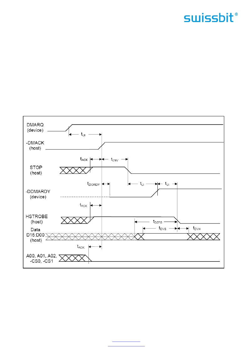
�e)� The� host� shall� negate� –� CS0,� -CS1,� DA2,� DA1,� and� DA0.� The� host� shall� keep� –� CS0,� -CS1,� DA2,� DA1,� and� DA0�
�negated� until� after� negating� –� DMACK� at� the� end� of� the� burst.�
�f)�
�Steps� I,� (d),� and� (e)� shall� have� occurred� at� least� t� ACK� before� the� host� asserts� –� DMACK.� The� host� shall� keep� –�
�DMACK� asserted� until� the� end� of� an� Ultra� DMA� burst.�
�g)� The� device� may� negate� –� DDMARDY� t� ZIORDY� after� the� host� has� asserted� –� DMACK.� Once� the� device� has� negated�
�–� DDMARDY,� the� device� shall� not� release� –� DDMARDY� until� after� the� host� has� negated� DMACK� at� the� end� of�
�an� Ultra� DMA� burst.�
�h)� The� host� shall� negate� STOP� within� t� ENV� after� asserting� –� DMACK.� The� host� shall� not� assert� STOP� until� after� the�
�first� negation� of� HSTROBE.�
�i)�
�j)�
�The� device� shall� assert� –� DDMARDY� within� t� LI� after� the� host� has� negated� STOP.� After� asserting� DMARQ� and� –�
�DDMARDY� the� device� shall� not� negate� either� signal� until� after� the� first� negation� of� HSTROBE� by� the� host.�
�The� host� shall� drive� the� first� word� of� the� data� transfer� onto� D[15:00].� This� step� may� occur� any� time� during�
�Ultra� DMA� burst� initiation.�
�k)� To� transfer� the� first� word� of� data:� the� host� shall� negate� HSTROBE� no� sooner� than� t� UI� after� the� device� has�
�asserted� –� DDMARDY.� The� host� shall� negate� HSTROBE� no� sooner� than� t� DVS� after� the� driving� the� first� word� of�
�data� onto� D[15:00].�
�Figure� 15:� Ultra� DMA� Data-Out� Burst� Initiation� Timing�
�Note:� The� definitions� for� the� STOP,� DDMARDY,� and� HSTROBE� signal� lines� are� not� in� effect� until� DMARQ�
�and� DMACK� are� asserted.�
�6.5.4.4.7� Sustaining� an� Ultra� DMA� Data-Out� Burst�
�An� Ultra� DMA� Data-Out� burst� is� sustained� by� following� the� steps� lettered� below.� The� timing� diagram� is� shown� in�
�Figure� 16:� Sustained� Ultra� DMA� Data-Out� Burst� Timing.� The� associated� timing� parameters� are� specified� in� Table� 27:�
�Ultra� DMA� Data� Burst� Timing� Requirements� and� are� described� in� Table� 28:� Ultra� DMA� Data� Burst� Timing�
��The� following� steps� shall� occur� in� the� order� they� are� listed� unless� otherwise� specifically� allowed:�
�a)� The� host� shall� drive� a� data� word� onto� D[15:00].�
�Swissbit� AG�
�Industriestrasse� 4�
�Swissbit� reserves� the� right� to� change� products� or� specifications� without� notice.�
�Revision:� 1.20�
�CH-9552� Bronschhofen�
�Switzerland�
�www.swissbit.com�
�industrial@swissbit.com�
�C-320_data_sheet_CF-HxBO_Rev120.doc�
�Page� 36� of� 101�
�发布紧急采购,3分钟左右您将得到回复。
相关PDF资料
SFCF4096H4BK2SA-I-QT-553-SMA
FLASH SLC UDMA/MDMA/PIO 4G
SFCF64GBH2BU4TO-I-NU-517-STD
FLASH SLC UDMA/MDMA/PIO 64GB
SFN08B4702CBQLF7
RES ARRAY 47K OHM 7 RES 8-DFN
SFP1050-12BG
FRONT END AC/DC 1050W 12V
SFP450-12BG
PWR SUP 450W 12V 36.6A W/STANDBY
SFSD1024N1BN1TO-I-DF-151-STD
FLASH MICRO SD CARD IND S-200 1G
SFSD2048L1BN2TO-I-DF-151-STD
FLASH SECURE DGTL CARD SD 2G
SFSD4096L1BN2TO-I-Q2-141-STD
FLASH SECURE DGTL CARD SDHC 4G
相关代理商/技术参数
SFCF2048H1BO2TO-I-M0-533-ZP1
制造商:SWISSBIT NA INC 功能描述:FLASH
SFCF2048H1BO2TO-I-M0-543-SMA
制造商:SWISSBIT NA INC 功能描述:FLASH
SFCF2048H2BU2TO-C-MS-527-STD
制造商:SWISSBIT NA INC 功能描述:FLASH
SFCF2048H2BU2TO-I-MS-517-STD
功能描述:FLASH SLC UDMA/MDMA/PIO 2GB RoHS:是 类别:存储卡,模块 >> 存储器,PC 卡 系列:C-440 标准包装:30 系列:- 存储容量:8GB 存储器类型:存储卡 - Extreme III SD?
SFCF2048H2BU2TO-I-MS-527-STD
制造商:SWISSBIT NA INC 功能描述:FLASH
SFCF2048H4BK1SA-C-QT-553-SMA
制造商:SWISSBIT NA INC 功能描述:FLASH
SFCF2048H4BK1SA-I-QT-553-SMA
功能描述:FLASH SLC UDMA/MDMA/PIO 2G RoHS:是 类别:存储卡,模块 >> 存储器,PC 卡 系列:C-300 标准包装:30 系列:- 存储容量:8GB 存储器类型:存储卡 - Extreme III SD?
SFCF2048H4BK2SA-C-DS-553-SMA
制造商:SWISSBIT NA INC 功能描述:FLASH SLC UDMA/MDMA/PIO 2G